Photo resist PCB making
From
photo resist PCB
Why do I want to make my PCB this way and not the toner transfer way:
Toner transfer is A very good way to make PCB's for micro controller board or small electronics circuits.
For High Frequency PCB's like this one, toner transfer is not really great. Imagine you have to fill up all those big squares and the full backside of the pcb as ground with toner. This is why I used photo resist PCB for this project.
If you have to make more than 1 PCB of the same design, this is much faster be course you don't have to do the printing and toner transfer thing every time again.
I've made A little test pcb first with A old piece of pcb material.
First you have to print you design on transparent sheet:
Warning: Make sure your printer can print on this material !!
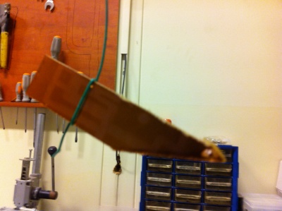
Put the sheet on the (old scanner) UV light And lay down you PCB over the part your designed.
Tip: write some text in your design so you now the sheet is not upside down.
Close the old scanner en turn on the light for about 3 minutes.
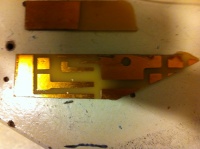
When you take out your PCB there is A yellow glow on it with the traces you made:
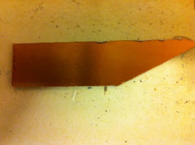
It's really hard to see on the picture but try it yourself and you will see.
Now we go to the part where you have to develop the PCB and prepare it for etching.
I've made A second tank for developing photo resistant PCB's.
It's filled with water and A little bit Natriumhydroxide (riool ontstopper).
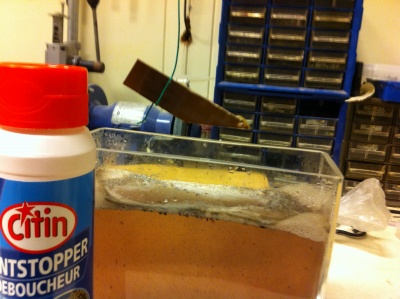
Dip the PCB in the second tank for about 2 second and see how the photo resist layer will come off.
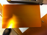
After this step the PCB is ready for etching: This is the normal procedure, dip the PCB in the etch tank for about 15 to 20 minutes and see the copper come off:
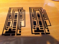
I've made several PCB's (16cmx10cm) this way and I have to say it works very well:
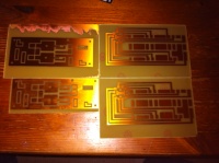
All with the back of the PCB filled with copper
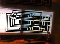
further experimenting (Duality)
I tried to make pcb's this way but did not have a clear sheet to print on
So i used a4 paper, had pretty good results, with a exposure time of betwee 3 and 4 minutes.
MichielB came with a link showing a4 drenched in oil, he made a sheet and I tried making a print with it,
after a lot of experimenting I found that a exposure time of two and half minute is the best.
It works really good!
(link to oil paper)
