Toner transfer PCB making
From
Contents
This page is intended to document the PCB making process at TkkrLab.
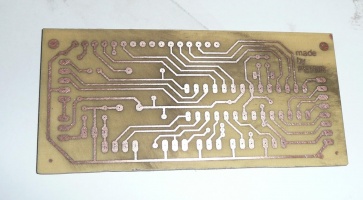
We are currently making our own PCB's using the toner transfer technique. The first test on juli 2011 failed. The cause of this was not enough toner on the PCB. It seems the toner density is too low when printing. I've created some files with PJL print commands to change the default density of our printer from 3 to 5, the maximum setting. This worked and finaly in december 2011 our first prints have been made:
Used hardware, tools and chemicals
- HP Laserjet 2100 with non original toner (printer set to maximum toner density)
- paper from Ikea magazine for printing and transfer of the toner
- ferric chloride (FeCl3) as etchant
- abrasive pad for cleaning PCB
- acetone for cleaning and removing toner from PCB
- waterproof felt pen (Schneider 222F OHP black) with 0.7mm tip for fixing small toner errors before etching
- Column drilling machine /dremel tool with PCB drills
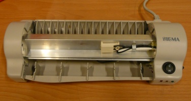
- laminator modified for pcb's:
Steps (quick version) to make a pcb:
The following steps describe in general how we make pcb's at TkkrLab. If you want to make your first PCB at TkkrLab it would be a good idea to first watch how its done by someone with some experience to see all details before trying it yourself.
- Make your pcb layout with your favorite tool (KiCad/eagle etc).
- Print it your layout on the HP Laserjet 2100 (for single side PCB just print normal but make sure any text in your layout is mirrored. For double sided PCB mirror the top layer before printing.
- cut a page from the Ikea folder to size (about 2..4 cm bigger (on each side) then the size of the intended pcb) and attach it on your just printed layout with heat resistant stickers.
- place the paper back into the printer (manual feed, straight trough) and print the layout again.
- carefully remove the ikea paper with layout from the underlaying paper and start preparing the pcb:
- take a blank piece of pcb and cut it to the right size.
- clean it with some water and the abrasive pad for several minutes. After that clean it with acetone on a clean cloth/kitchenpaper and do not touch the copper anymore.
- Place your layout on top of the copper and fix it on the backside, again with heat resistive stickers.
- Heat up the laminator (make sure it is heated before start, this can take up to 15 minutes
- For the transfer of the toner take the pcb (copper side on top) and run it trough the laminator 10 times (if the laminator stops running turn it off and on again and continue).
- Turn off the laminator and let the pcb with paper cool down.
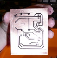
- Place the pcb in a bucket of hand warm water until the paper is weak enough so it almost falls off. You can rub very gently with your fingertips until all paper is gone. Your pcb should now look something like this:
- Any open/bad spots can be manually repared with the water resistant felt pen.
- if your pcb looks ok you can finaly etch it in the ferric chloride etch tank.
- use the heaterplate to warm up the tank for faster etching, also moving the pcb around or wiggling the etch tank quickens the process. check the pcb every few minutes to see if its done yet (it takes between 25..40 minutes to complete the process).
- clean the PCB and dry it. The toner on the traces can be removed with acetone
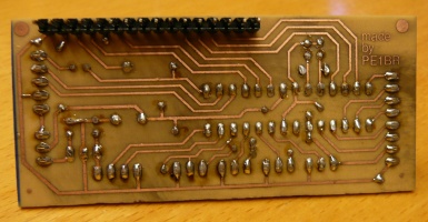
- Finaly you can drill the necessary holes to complete the pcb.
Links with useful information
- Copper Chloride in Aqueous Hydrochloric Acid Solution fast Etchant using cheap but dangerous chemicals
- Direct inkjet to PCB printing yahoo group
- Homebrew PCB yahoo group with a lot of info about used printers/toners/technique etc.
- laser, inkjet and hybrid PCB making with a lot of info including a list of compatible epson inkjet printers
- table (german language) with used printers/transfer paper/temperature/laminator
- Tutorial with pics toner transfer method explained in detail
- another toner transfer method (in german)
- Laminator temperature control modification with avr
